Research Areas
Nanophotonics & Nanoplasmonics
Reseach topics
Single nanohole & photonic crystal
Single
nanohole as nonlinear element
Publications
Single nanohole as nonlinear element
Optical Tamm states
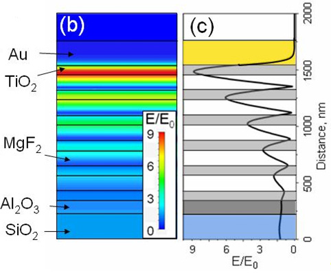 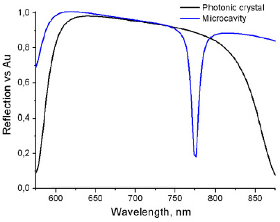 |
The ОТS is an optical analog of an electronic Tamm state (OTS).The OTS can arise at the interface between a photonic crystal and a metal. The physical reasons for the localization of the electromagnetic field of the OTS at the interface are (а) an exponential decay of the field toward the medium with a negative dielectric permittivity (the imaginary value of the wave vector in the medium) and (b) a decrease of the wave in the medium with a positive dielectric permittivity because the condition of total internal reflection is implemented. Over the last few years, OTS have been intensively studied both theoretically and experimentally. Figure (a) shows the experimental arrangement to create OTS. A 12-layer periodic dielectric structure (metamaterial) is deposited on a quartz substrate (which is shown at the top in Figure). The dielectric structure consists of an Al2O3 layer (with a thickness of 125 nm) and alternating TiO2 and MgF2 layers (with their thicknesses being 82 and 125 nm, respectively). A gold film with a thickness of 220 nm is deposited on the surface of the metamaterial (at the “bottom” in Figure). Since the thickness of this film considerably exceeds the thickness of the skin layer (~80 nm), the film is opaque in the wavelength range of the incident light (from 575 to 875 nm). Figure (b) shows a computer simulation by the FDTD method of the spatial distribution of the electromagnetic field of the OTS, and (с) its transverse section. Referenses:
|
Single Nanohole, Photonic crystal & Microcavity
|
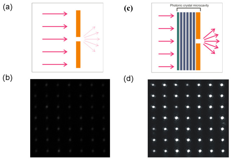
Transmissions of nanoholes in the Au film and nanoholes in the photonic crystal microcavity at identical parameters of illumination and detection at a light wavelength nearby the PCM’s resonance mode: Left column – nanoholes in the Au film: (a) the scheme of nanoholes illumination in the reference Au film, (b) nanoholes images of the reference Au film in the 2D CCD of the microscope, Right column – nanoholes in the photonic crystal microcavity: (c) the scheme of nanoholes illumination in the photonic crystal microcavity, (d) nanoholes images of the photonic crystal microcavity in the 2D CCD of the microscope. |
For
the
first time we have
demonstrated an approach to control transmission of light through a
single nanohole with the use of photon crystal microcavity. By use of
the approach 28-fold enhanced transmission of light through a single
nanohole in Au film has been experimentally demonstrated. The approach
has the following advantages: (1) it enables to considerably increase
transmission of light through a single nanohole, (2) the increase in
transmission is unaffected by the hole diameter, (3)
the transmission of nanohole is selective in frequency, the width of
the resonance ~λ/90, (4) no auxiliary structures are
necessary
on the surface of the Au film (extra nanoholes, grooves, etc.). Referenses:
|
Institute for spectroscopy RAS, Fizicheskaya Str., 5, Troitsk, Moscow, 142190 Russia
phone: +7 495 851-02-33
e-mail: atom.nano.optics@gmail.com