Research Areas
Reseach topics
Nanophotonics & Nanoplasmonics
Publications
Atom nanolithography
|
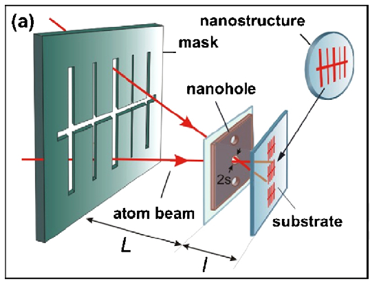
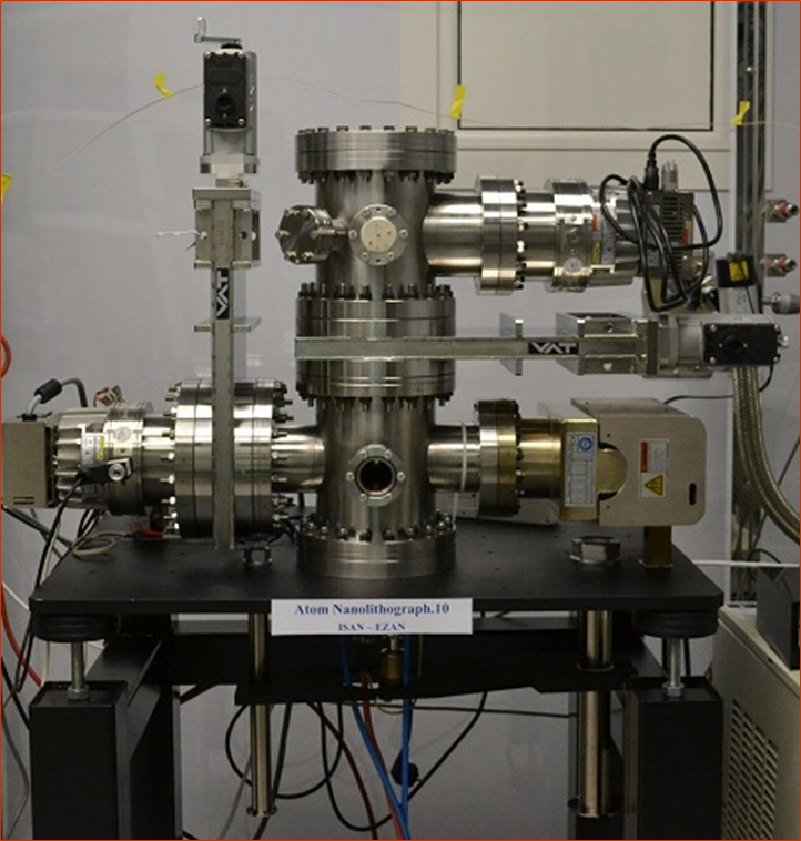
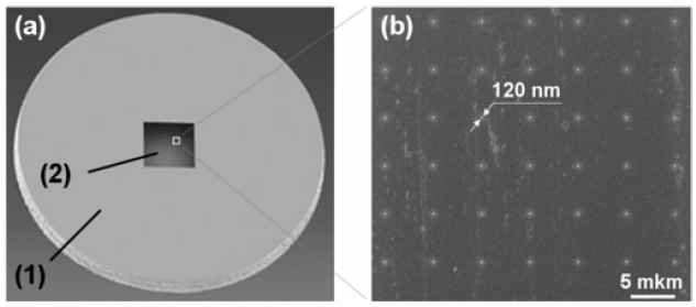
Principal scheam of atom pinhole camera "Atom Nanolithoraph" based on atom pinhole camera. Prototype of a comertial device builled in collaboration of Institute for spectroscopy and Experimental Factory of Scientific Engineering
(1) membrane holder in the form of a disc 3 mm in
diameter and 200 μm in
AFM-image of a nanostructure built up from atoms of In on a silicon surface
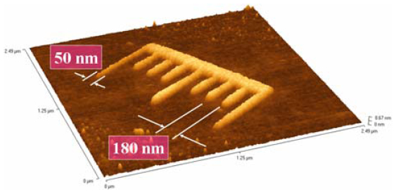
Plasmonic nanowaveguide |
There
are several
approaches to fabrication of nanostructures with sizes of several tens
of
nanometers; each of them has a number of advantages and drawbacks. In
particular, the difficulties in further development of approved methods
are
well known: (i) conventional photolithography has a diffraction limit,
(ii)
lithography based on charged particle beams meets problems related to
commercial production of structures and a significant role of Coulomb
repulsion, (iii) scanning probes have a low output, and (iv) self
assembling
fabrication is not an universal process. An alternative approach for
nanotechnology is atom optics, i.e., optics of material particles
(electron and
ion optics). It deals with problems of
formation and control of
ensembles and
beams of neutral atoms. The term “atom optics” is
similar to the terms “light
optics” or “photon optics”. An important
direction of atom optics is the
development of basic elements, similar to the elements of conventional
light
optics. Among many applications of atom optics elements, atom
lithography is
potentially important for micro and nanofabrication of material
structures. Despite a large number of proposed methods for focusing atomic beams, this problem remains experimentally difficult. The main difficulty is the fabrication of the atom–field interaction potential with properties similar to those of the “ideal” lens for atoms. We experimentally implemented for the first time another approach to the problem of focusing and constructing images in atomic optics, which is based on the concept of a pinhole camera; the latter is used both in light optics and in modern experimental physics when it is difficult to form a focusing potential. In an atomic “pinhole camera”, an atomic beam is transmitted through an array of holes in a mask, thus forming, by analogy with optics, a “luminous object” of specified geometry. The atoms transmitted through the holes in the mask, propagating in vacuum over straight-line trajectories, arrive at a thin film located at a distance L from the mask. Each hole of the film serves as a pinhole camera for atoms, forming an image of the “object” on the surface of a substrate, which is located at a small distances l behind the film. In this geometry, a set of object images, decreased approximately by a factor of m = L/l , is formed on the substrate. The atomic “pinhole camera” is an analog of the Feynman’s scalable manufacturing system [1] that could manufacture a smaller scale replica of itself. References: [1] Feynman R P 1993 Infinitesimal machinery J. Microelectromech. Syst. 2, 4–14 (1983 Lecture reprinted)
|
Institute for spectroscopy RAS, Fizicheskaya Str., 5, Troitsk, Moscow, 142190 Russia
phone: +7 495 851-02-33
e-mail: atom.nano.optics@gmail.com